
Datasheet
PTX105R
NFC Reader IC
PTX105R Datasheet v1.1
Jun 11, 2024
Page 1
© 2024 Renesas Electronics
Product Description
The PTX105R is a highly integrated NFC reader IC for
contactless communication, which is optimized for
reader performance and interoperability. While
eliminating EMC filter and matching components,
the PTX105R enables simple integration and
compact design without the complexity associated
with existing solutions (dual resonating circuits
composed by EMC filter and antenna).
Due to its modular Soft Controller architecture, the
NFC functionalities are integrated into a split stack
solution where time-critical operations are running
on the on-chip MCU, and the rest of the NFC logic is
in the host controller to carry out applications such
as IoT reader.
Features
The architecture enables:
• Efficient power transmission with accurate
digital programmability of RF carrier and
modulation shape
• EMC filter removal due to sinewave output
driver and Direct Antenna Connection (DiRAC)
• -80dBc RX sensitivity with full input dynamic
range due to DiRAC
• SDK composed of FW and SW integrated in a
Split Stack architecture with Over-The-Air
firmware update on the host processor:
- Modular SW stack running on the Host
architecture
- Integrated FW running on the on-chip MCU
for timing critical operations
• Fractional-N PLL to support any reference input
clock frequency from 13.15MHz to 52MHz
• ISO/IEC14443-A reader/writer mode up to
848kBit/s
• ISO/IEC14443-B reader/writer mode up to
848kBit/s
• NFC Forum reader/writer mode
• Supports reading/writing of NFC Tag Type 2, 3,
4A/4B and 5
1
MIFARE is a registered trademark of NXP B.V
• FeliCa reader/writer mode 212&424kBit/s
• ISO/IEC 15693 reader/writer mode
• Support reading/writing of Mifare
®
card family
including Mifare Classic
®
(without crypto)
1
• Support Apple ECP “Enhanced Contactless
Polling” (feature only available for customers
with valid Apple MFi license)
• Transparent mode allowing implementation of
customer protocols based on low-level
commands
• NFC Forum P2P Passive Initiator
• NFC Card Emulation Mode for Tag Type 4A
(106kBit/s)
• Low Power Card Detection (LPCD)
• Low Power Field Detection (LPFD)
• Programmable GPIOs
• Supported host interfaces: I2C, SPI, UART
PTX105R reader IC enables key improvements in
customer care-about such as:
RF performance: Patented groundbreaking
architecture enables efficient power transmission
and -80dBc RX sensitivity, state of the art reader
performance even in challenging and complex
integration environments.
Interoperability:
• Digitized architecture enables accurate shape
control of the modulated signal.
• Elimination of the EMC filter results in well-
behaved signal shape avoiding overshoot and
undershoot
• DiRAC allows minimum output power loss on
matching structure with high input sensitivity,
which translates to substantially larger
operating volume.
Manufacturability:
• No need for bulky and performance-limiting
external components of the EMC filter (no
tolerances issue introduced) minimizing the
performance variation between final devices.

PTX105R Datasheet
PTX105R Datasheet v1.1
Jun 11, 2024
Page 2
• Reduced number of matching components
allow lower antenna matching impedance,
resulting in higher output power.
• Accurate adjustment of transmitter and
receiver parameters due to digital architecture
enabling tighter production control giving more
margin for new use cases.
PTX105R is optimized for applications such as IoT
Reader, Access Control, Gaming, Transportation,
Wearables etc.

PTX105R Datasheet
PTX105R Datasheet v1.1
Jun 11, 2024
Page 3
Figure 1: Block Diagram

PTX105R Datasheet
PTX105R Datasheet v1.1
Jun 11, 2024
Page 4
Contents
1. Pinning Information ....................................................................................................................... 7
1.1 Pin Diagram ............................................................................................................................ 7
1.2 Pin Description ....................................................................................................................... 7
2. Electrical Characteristics .............................................................................................................. 9
2.1 Absolute Maximum Ratings ................................................................................................... 9
2.2 Electrical Characteristics ...................................................................................................... 10
3. Functional Description ................................................................................................................ 12
3.1 System Architecture ............................................................................................................. 12
3.2 Power Management ............................................................................................................. 12
3.2.1. Power Supply Concept .......................................................................................... 12
3.2.2. SEN-Pin ................................................................................................................. 13
3.2.3. Supply Ramp-Up Sequence .................................................................................. 13
3.2.4. Energy States ........................................................................................................ 14
3.3 Clock Concept ...................................................................................................................... 15
3.3.1. Low Power Oscillator (LPO) .................................................................................. 15
3.3.2. Crystal Oscillator (XTAL) ....................................................................................... 15
3.3.3. External Reference Clock ...................................................................................... 15
3.3.4. Phase Lock Loop (PLL) ......................................................................................... 15
3.4 Contactless Interface ........................................................................................................... 15
3.4.1. Analog/Digital Transmitter ..................................................................................... 16
3.4.2. Analog/Digital Receiver ......................................................................................... 16
3.4.3. Polling Loop ........................................................................................................... 17
3.4.4. Low Power Card Detection (LPCD) ....................................................................... 17
3.4.5. Low Power Field Detection (LPFD) ....................................................................... 17
3.4.6. Wave-Shaping ....................................................................................................... 17
3.4.7. Digital Dynamic Power Control (DDPC) ................................................................ 18
3.5 Other Supported Features ................................................................................................... 18
3.5.1. Over-Temperature Protection ................................................................................ 18
3.5.2. Auxiliary Digital-to-Analog Converter (AUS-DAC) ................................................. 18
3.5.3. GPIO Customer Usage .......................................................................................... 18
3.6 Programmable Control Logic ............................................................................................... 18
3.6.1. On-chip MCU ......................................................................................................... 19
3.6.2. PTX105R device control firmware ......................................................................... 19
3.7 Host Interface ....................................................................................................................... 19
3.7.1. Host-Interface Selection ........................................................................................ 19
3.7.2. Host-Interface Lines............................................................................................... 19
3.7.3. Host Interface Protocol .......................................................................................... 20
3.7.4. IRQ ......................................................................................................................... 20
3.7.5. SPI ......................................................................................................................... 20
3.7.6. I2C ......................................................................................................................... 21
3.7.7. UART ..................................................................................................................... 22
3.8 FW/SW Functionality ............................................................................................................ 22
3.8.1. NSC-Interface ........................................................................................................ 22

PTX105R Datasheet
PTX105R Datasheet v1.1
Jun 11, 2024
Page 5
3.8.2. SW Split Stack ....................................................................................................... 22
4. Reference Schematic ................................................................................................................... 24
5. Ordering and Package Information ............................................................................................ 25
5.1 Ordering Information ............................................................................................................ 25
5.2 Package Marking.................................................................................................................. 25
5.3 Package Drawing and Dimension ........................................................................................ 26

PTX105R Datasheet
PTX105R Datasheet v1.1
Jun 11, 2024
Page 6
List of Figures
Figure 1: Block Diagram ........................................................................................................................... 3
Figure 2: Pin Diagram .............................................................................................................................. 7
Figure 3: System Architecture for IoT Application .................................................................................. 12
Figure 4: Supply Ramping Up (SEN at logic-low) .................................................................................. 13
Figure 5: Supply Ramp Up (SEN==VCC) .............................................................................................. 14
Figure 6: Contactless Interface .............................................................................................................. 16
Figure 7: Dynamic Digital Power Control (DDPC) ................................................................................. 18
Figure 8: SPI mode 0 (CPOL, CPHA = 0) .............................................................................................. 21
Figure 9: PTX105R SW Stack Integration View ..................................................................................... 23
Figure 10: Exemplary Reference Schematic ......................................................................................... 24
Figure 11: Package Marking Drawing .................................................................................................... 25
Figure 12: Package Drawings and Dimensions ..................................................................................... 26
List of Tables
Table 1: Pin Description ........................................................................................................................... 8
Table 2: Absolute Maximum Ratings ....................................................................................................... 9
Table 3: Operating Range ...................................................................................................................... 10
Table 4: DC characteristics .................................................................................................................... 10
Table 5: Receiver / Transmitter Characteristics ..................................................................................... 11
Table 6: Reference Input Frequency Requirements .............................................................................. 11
Table 7: Crystal Requirements ............................................................................................................... 11
Table 8: Host Interface Selection ........................................................................................................... 19
Table 9: Pin Assignment for HIF Selection ............................................................................................ 20
Table 10: SPI Timing Characteristics ..................................................................................................... 21
Table 11: I2C Address Selection depending on HIF Pin Setting ........................................................... 22
Table 12: Reference Schematic Components ....................................................................................... 24
Table 13: Ordering Information .............................................................................................................. 25
Table 14: Marking Code HVQFN56 ....................................................................................................... 25

PTX105R Datasheet
PTX105R Datasheet v1.1
Jun 11, 2024
Page 7
1. Pinning Information
1.1 Pin Diagram
56 55 54 53 52 51 49 48 47 46 45 44 43
15 16 17 18 19 20 21 22 23 24 25 26 27
50
28
01
02
03
04
05
06
07
08
09
10
11
12
13
14
42
41
40
39
38
37
36
35
34
33
32
31
30
29
VCC
VCC
VCC
VCC
SEN
VCC
DNC
VDDIO
IRQ
SIF1
SIF2
D18VD
GPIO12
GPIO11
GPIO10
GPIO9
HIF1
GND
DNC
XIN
XOUT
HIF2
DNC
HIF3
DNC
DNC
GPIO8
GPIO7
DNC
DNC
DNC
DAC_O
VCC
VCC
TRXp
TRXp
TRXn
TRXn
VCC
VCC
DNC
DNC
DNC
DNC
DNC
DNC
DNC
DNC
VDDIO
DNC
DNC
DNC
GND
HIF4
GPIO5
GPIO6
PTX105R
QFN56
Figure 2: Pin Diagram
1.2 Pin Description
Signal Name
Signal Type
QFN56 Pin
Description
DNC
-
1-3
Do not connect
DAC_O
Analog out
4
AUX-DAC output voltage
VCC
Supply
5
NFC IC supply
VCC
Supply
6
NFC IC supply
TRXp
Analog inout
7
Transmitter/Receiver pin p
TRXp
Analog inout
8
Transmitter/Receiver pin p
TRXn
Analog inout
9
Transmitter/Receiver pin n
TRXn
Analog inout
10
Transmitter/Receiver pin n
VCC
Supply
11
NFC IC supply
VCC
Supply
12
NFC IC supply
DNC
-
13-20
Do not connect
VDDIO
Supply
21
IO Pad supply
DNC
-
22
Do not connect
DNC
-
23
Do not connect
DNC
-
24
Do not connect
GND
Supply
25
Ground
HIF4
Digital inout
26
SPI: MISO, I2C: SCL, UART: TXD
GPIO5
Digital inout
27
General purpose digital IO pin
GPIO6
Digital inout
28
General purpose digital IO pin
GPIO7
Digital inout
29
General purpose digital IO pin

PTX105R Datasheet
PTX105R Datasheet v1.1
Jun 11, 2024
Page 8
GPIO8
Digital inout
30
General purpose digital IO pin
DNC
-
31
Do not connect
DNC
-
32
Do not connect
HIF3
Digital inout
33
SPI: MOSI, I2C: SDA, UART: RXD
DNC
-
34
Do not connect
HIF2
Digital inout
35
SPI: SCK, I2C: ADDR1, UART: RTS
XOUT
Analog out
36
Xtal oscillator output
XIN
Analog in
37
Xtal oscillator input / Reference clock input
DNC
-
38
Do not connect
GND
Supply
39
Ground
HIF1
Digital inout
40
SPI: NSS, I2C: ADDR0, UART: CTS
GPIO9
Digital inout
41
General purpose digital IO pin
GPIO10
Digital inout
42
General purpose digital IO pin
GPIO11
Digital inout
43
General purpose digital IO pin
GPIO12
Digital inout
44
General purpose digital IO pin
D18VD
Supply
45
Decoupling of core supply
SIF2
Digital in
46
Select interface type bit 2
SIF1
Digital in
47
Select interface type bit 1
IRQ
Digital out
48
Interrupt request to host
VDDIO
Supply
49
IO Pad supply
DNC
-
50
Do not connect
VCC
Supply
51
NFC IC supply
SEN
Analog in
52
System enable input
VCC
Supply
53
NFC IC supply
VCC
Supply
54
NFC IC supply
VCC
Supply
55
NFC IC supply
VCC
Supply
56
NFC IC supply
GND
Supply
-
The exposed pad at the back of QFN is used as
GND
Requires good thermal connection to ensure low
thermal resistance for power dissipation
Table 1: Pin Description

PTX105R Datasheet
PTX105R Datasheet v1.1
Jun 11, 2024
Page 9
2. Electrical Characteristics
2.1 Absolute Maximum Ratings
Symbol
Parameter
Conditions
Min
Typ
Max
Unit
Remarks
V
CC
Supply voltage at VCC
-0.5
5.5
V
T
J
Junction temperature
-40
125
°C
T
S
Storage temperature
-40
150
°C
R
th(ja)
Thermal resistance
junction to air
29
K/W
Based on
JESD-51
P
TOT
Total power dissipation
allowed in the chip
1.4
W
V
ESD(HBM)
electrostatic discharge
voltage; Human Body
Model (HBM)
1500 Ohm, 100 pF;
JEDEC JS-001-2017
Table 2A
1500
V
All pins
except
TRXp/n
V
ESD(HBM),TRX
electrostatic discharge
voltage; Human Body
Model (HBM)
1500 Ohm, 100 pF;
JEDEC JS-001-2017
Table 2A
750
V
ESD-
sensitive
pins:
TRXp/n
V
ESD(CDM)
electrostatic discharge
voltage (Charge
Device
model)
Field induced model;
JEDEC JS-002-2018
1000
V
I
LU
Latch up
AEC-Q100
(Transient current)
100
mA
V
inmax
Maximum input
voltage at digital IO
pins
-0.3
V
DDIO
+0.3
V
I
iomax
Maximum current into
digital IO pins
4
mA
Table 2: Absolute Maximum Ratings

PTX105R Datasheet
PTX105R Datasheet v1.1
Jun 11, 2024
Page 10
2.2 Electrical Characteristics
Unless noted otherwise, typical condition T
A
=25°C, V
cc
= 5.4V, F
ref_clk
= 27.12MHz, V
ref_clk
=1.8Vpp.
Symbol
Parameter
Conditions
Min
Typ
Max
Unit
Remarks
T
A
Ambient temperature
-40
85
°C
T
J
Junction temperature
-40
120
°C
V
CC
Supply voltage
2.7
5.5
V
V
DDIO
Pad supply voltage
1.62
5.5
V
V
SEN_H
System Enable (SEN) pin
high-level voltage range
1.62
V
CC
V
V
IH
GPIO pins high level input
voltage
0.75*V
DDIO
V
DDIO
V
V
IL
GPIO pins low level input
voltage
0
0.15*V
DDIO
V
V
OH
GPIO pins high level
output voltage
2
V
DDIO
-0.5
V
DDIO
V
V
OL
GPIO pins low level
output voltage
0
0.45
V
Table 3: Operating Range
Symbol
Parameter
Conditions
Min
Typ
Max
Unit
Remarks
I
PD
Power down current
consumption
V
cc
= 3.6V SEN=0
3
uA
I
STBY
Standby current
consumption
V
cc
= 3.6V
15
uA
I
CD_rd
Low power card
detection current
consumption
V
cc
= 5.5V
100
uA
2Hz polling
frequency with
optimized
reading
distance
I
VCC
Supply current
500
mA
Table 4: DC characteristics
2
VOH measurement condition: Iload=2.8mA with VDDIO=4.5V; Iload=0.4mA with VDDIO=1.62V.
VOL measurement condition: Iload=2.1mA with VDDIO=4.5V; Iload=0.6mA with VDDIO=1.62V.

PTX105R Datasheet
PTX105R Datasheet v1.1
Jun 11, 2024
Page 11
Symbol
Parameter
Conditions
Min
Typ
Max
Unit
Remarks
V
in_rx_rd
RX carrier signal reader
100m
50
Vpp
differential
S
in_RX_rd
RX sensitivity AM
-80
3
dBc
V
in_rx_rd
≥25Vpp
H
out_tx_rd
Transmitter output
harmonics
-60
dBc
C
out_tx
Transmitter serial
output capacitance
640
pF
Table 5: Receiver / Transmitter Characteristics
Symbol
Parameter
Conditions
Min
Typ
Max
Unit
Remarks
F
ref_clk
Reference clock input
frequency
13.15
27.12
52
MHz
V
ref_clk_low
Reference clock input
voltage low
0
400
mV
V
ref_clk_high
Reference clock input
voltage high
1.4
1.95
V
Δf
ref_clk
Reference clock frequency
tolerance
-50
+50
ppm
DC_f
ref_clk
Reference clock duty cycle
40
50
60
%
Table 6: Reference Input Frequency Requirements
Symbol
Parameter
Conditions
Min
Typ
Max
Unit
Remarks
F
xtal_clk
Reference clock
input frequency
27.12
MHz
Δf
xtal_clk
Reference clock
frequency tolerance
-50
+50
ppm
ESR
Equivalent serial
resistance
150
Ohm
C
L
Load capacitance
6
pF
On chip
available
Table 7: Crystal Requirements
3
To achieve -80dBc RX sensitivity, V
CC
shall not have voltage ripple higher than 500uVrms (V
VDPA
= 5V) around the carrier
frequency (±1MHz).

PTX105R Datasheet
PTX105R Datasheet v1.1
Jun 11, 2024
Page 12
3. Functional Description
3.1 System Architecture
PTX105R is a highly integrated reader IC using a split-stack SW architecture, allowing flexible adaption
of SW to the needs of the application system such as IoT/NFC Reader. This flexibility is achieved by an
optimized software interface and ready to use SW-stack for the host-controller. The portable SW stack
written in C, implements high level NFC functionality and provides easy to use APIs for integration into
the Host system.
Figure 3 shows PTX105R used for IoT application as an example. Timing critical tasks such as polling
and protocol handling are executed directly by PTX105R Hardware, while higher-level protocol related
tasks are executed by the SW stack running on the Host processor.
Application
processor
Application Data
IoT Application
Application
Data Partioning
NFC-HW
NFC-FW
PTX105R Split
-Stack
-Solution
Split-Stack-
Implementation
Application
view
L4-Protocol
L3-Protocol
L2-Interface
PHY-RF-Interface
PTX105R IC
Host
Figure 3: System Architecture for IoT Application
The PTX solution is modular and runs on different platforms, providing additional facilities for custom
features in case needed.
3.2 Power Management
The power management unit is the central circuit of the PTX105R responsible for providing all necessary
reference voltages and currents, generating the internal supply domains, implementing the power-up
sequence, and controlling the transitions between different energy states.
3.2.1. Power Supply Concept
PTX105R has 3 externally accessible supply domains which are described as follows:
3.2.1.1. VCC
VCC is the main supply domain from which all functional blocks are supplied. To operate the IC this
supply must always be present.
PTX105R Datasheet
PTX105R Datasheet v1.1
Jun 11, 2024
Page 13
3.2.1.2. D18VD
The internally generated core supply is routed to pin D18VD for external supply blocking. Hence external
supplies are not allowed to be connected. For recommended blocking components please refer to the
relevant application note.
3.2.1.3. VDDIO
Pad supply for all GPIO- and HIF/SIF-pins. It must be present during start-up for proper host-interface
selection and afterward for host interface communication. In power-down mode, the voltage may be
removed from this domain, but the pin shall not be pulled to VS (i.e. to be put to HiZ).
If for power saving reasons at any point in time the VCC domain is switched off, then VDDIO must also
be removed.
3.2.2. SEN-Pin
The SEN-pin is used to boot up the PTX105R (logic-high level) or to bring the IC into power-down state
(logic-low level). Detailed ranges for the logic-levels are given in Table 3.
Note that SEN-input voltage must never exceed V
CC
. For safe operation, SEN shall change to a logic
low before V
CC
drops below V
CC_min
(value defined in Table 3).
Logic-low level pulses with smaller than 3.4 us pulse width on SEN-pin will not change the current energy
state of the IC. Negative pulses that are slightly longer will first reset the internal state and for even
longer negative pulses the IC changes the energy state to power-down mode. The exact pulse width
below which a reset is triggered, and above which power-down mode is entered depends on the blocking
capacitor value on D18VD-pin.
3.2.3. Supply Ramp-Up Sequence
For the supply ramp-up two sequences are proposed: a default sequence with SEN pin at logic-low for
relaxed timing constraints between V
CC
and V
DDIO
, and a sequence with SEN pin connected to VCC for
simpler configuration and faster start-up.
Ramp-up sequence with SEN at logic-low (transition into power-down mode):
• First, the battery supply V
CC
shall be ramped up – the IC remains in power-down mode
• V
DDIO
shall be ramped up. V
DDIO
may ramp concurrently to V
CC
.
• V
DDIO
supply and a stable state of SIF1/SIF2 pins shall latest be available when the SEN pin
voltage reaches a valid logic-high level. These timings also apply when leaving power-down
mode with disabled V
DDIO
.
V
t
V
CC
V
DDIO
SEN
V
SEN_min
SIF1/2
X/Z
00b/01b/10b
>= 0
Figure 4: Supply Ramping Up (SEN at logic-low)

PTX105R Datasheet
PTX105R Datasheet v1.1
Jun 11, 2024
Page 14
Ramp-up sequence with SEN at logic-high (transition into full-power mode):
• First, the battery supply V
CC
together with SEN pin voltage shall be ramped up.
• V
DDIO
shall be ramped and shall be at V
DDIO_min
latest 100 us after V
CC
exceeds V
CC_min
(i.e. 2.7
V). Latest at this point also the state of the SIF1/SIF2 pins shall be stable.
V
V
CC
V
DDIO
SEN
max 100us
V
DDIO_min
SIF1/2
X/Z
00b/01b/10b
t
Figure 5: Supply Ramp Up (SEN==VCC)
In typical applications, after SEN, V
DDIO
and SIF pins reach their stable level, PTX105R is ready for
operation in less than 1ms.
As SIF pins select the interface to be used and are only captured at boot time, it is important that the
logic level of SIF pins is set at the right time during the power-up process.
3.2.4. Energy States
To support the implementation of flexible system power consumption profiles, PTX105R offers different
energy states, each being a trade-off between functionality and power consumption.
3.2.4.1. Full-Power Mode
This is the main operating mode of PTX105R, in which all internal supply domains are ramped up and
all internal clocks are running. This mode is activated by applying a logic-high level at SEN-pin.
In this mode, PTX105R is fully active and can communicate with the host controller via the host
interface.
3.2.4.2. Power-Down (PD) mode
For maximum power saving PTX105R can be set to power-down mode by applying a logic-low level at
the SEN pin. In this mode PTX105R consumes its lowest power and does not react to any external
events. All GPIO-pins and the SIF1/SIF2-pins are switched to HiZ-state, the VDDIO supply may be
removed as well.
After leaving this mode the internal state of PTX105R is reset.
3.2.4.3. Standby (STBY) Mode
PTX105R supports Standby Mode for low power applications, with the possibility to wake up in response
to selected events such as Low Power Card Detection or Host-interface activities. In this mode, a logic-
high level shall be maintained on SEN-pin and the internal state of PTX105R is fully maintained.

PTX105R Datasheet
PTX105R Datasheet v1.1
Jun 11, 2024
Page 15
Depending on the application, different wake-up sources (e.g., execution of Polling loop, LPCD/LPFD
procedure) can be defined by the customer. Once configured, it runs autonomously and no interaction
with the Host is required.
Events triggering the wakeup of the IC from standby mode include:
• Activity on Host-interface
• Execution of Polling
• LPCD/LPFD procedure
3.3 Clock Concept
In PTX105R a low-power oscillator (LPO), a crystal oscillator (XO) and a phase-locked loop (PLL) are
the main blocks responsible for generating the necessary internal clocks in the various modes.
The reference clock for PTX105R can either be provided from an external clock source or the internal
crystal oscillator can be employed. Out of this clock, the PLL subsequently derives the system frequency
of 13.56MHz.
3.3.1. Low Power Oscillator (LPO)
The low-power oscillator is the lifeline of PTX105R, and its 125kHz-clock is particularly employed during
IC ramp-up and in standby mode, when the internal PLL is powered down to save energy.
3.3.2. Crystal Oscillator (XTAL)
The internal crystal oscillator is designed for crystal types with a resonant frequency of 27.12MHz,
which shall be externally connected between XIN- and XOUT pins. The oscillator will also work with
other crystals around this frequency - please contact Renesas for support.
The PTX105R features internal caps of 6pF each from XIN- and XOUT-pins to GND to act as crystal
load capacitors.
3.3.3. External Reference Clock
Alternative, an external reference clock with frequency between 13.15MHz and 52MHz can be applied
to XTAL1 pin. Detailed requirement on the external reference clock is specified in Table 6.
3.3.4. Phase Lock Loop (PLL)
A fractional-N PLL produces the core clock that is used to derive all the needed internal clocks.
A Delta-Sigma Modulator (DSM) is used to program the N division word of the fractional-N PLL. This
allows very fine frequency resolution of all clocks and output frequencies.
3.4 Contactless Interface
In PTX105R, lower-level functionality up to communication framing is available through the Contactless
Frontend, higher level functionality is implemented via the RF-Subsystem of the on-chip MCU (see 3.6.1)
Figure 6 gives a block level overview of the Contactless Interface. At TRXp / TRXn pins the device is
connected via a matching network to the antenna of the system.

PTX105R Datasheet
PTX105R Datasheet v1.1
Jun 11, 2024
Page 16
Analog
Receiver
Digital
Receiver
Analog
Transmitter
Digital
Transmitter
Low Power Card
Detection
Contactless
Interface
TRXp
TRXn
On-Chip
MCU
RF-
Subsystem
Low Power Field
Detection
Figure 6: Contactless Interface
3.4.1. Analog/Digital Transmitter
the RF-carrier according to the selected communication type.
The analog transmitter itself consists of a digital-like topology, which allows to directly output sinusoidal
carriers with high spectral purity and high efficiency. Therefore, EMC-filters, which are required in
conventional products in the matching network of Reader-antennas, can be omitted. Additionally, direct
antenna connection allows to shape the modulation in a very fine granularity. PTX105R offers dynamic
wave-shaping feature, which optimizes the modulation shapes to fulfill the requirements of the final
application – see chapter 3.4.6 for details.
The digital transmitter is responsible for encoding the command/data to be sent, applying the respective
modulation according to the selected communication type and synchronization of the modulation with
the carrier.
Output power of the transmitter can be adapted directly by adjusting the sinusoidal amplitude based on
the Received Signal Strength Indicator (RSSI). More details on Digital Dynamic Power Control (DDPC)
is explained in 3.4.7.
3.4.2. Analog/Digital Receiver
The receiver, consisting of an analog and a digital part, is responsible for reception, demodulation and
signal processing of incoming commands and data from the communication counterpart of PTX105R.
The analog receiver is based on an I/Q-architecture in the RF-domain, which is followed by a baseband
chain with programmable gain amplifiers and filters to properly adjust the received signal from varied
sized antennas to the full-scale range of the ADC.
The digital receiver provides means to configure the digital detection threshold on a fine granularity to
optimize sensitivity while having ensured good noise immunity. The received information is then
extracted on a bit- and frame-level to finally obtain the transmitted command/data.
For easy integration into the customer application, parameters such as PGA gain and digital RX-
threshold can be adapted based on the target applications, while RF-protocol related parameters such
as filter frequency settings stay pre-defined and unmodified.

PTX105R Datasheet
PTX105R Datasheet v1.1
Jun 11, 2024
Page 17
3.4.3. Polling Loop
Polling loop is the center of all NFC-applications. In a loop PTX105R executes polling sequences
through the defined RF-protocol following well-defined timing specifications. Depending on the use-
case, PTX105R can be configured to execute one of the two different scenarios as described below:
• Standard NFC applications, which polls for selected technologies in defined intervals. Between
the polling cycles PTX105R either stays idle or enters standby to reduce power consumption
• Low-Power application. For Reader applications, the Low-Power-Card-Detection mechanism is
used to significantly reduce power consumption (see chapter 3.4.4 for more information).
For applications where Host-Card-Emulation functionality is required, Low-Power-Field-Detection
can be enabled during Standby mode to detect the existence of an external RF field (see Chapter
3.4.5 for more information).
Polling interval together with the above-mentioned RF-protocol configurations can be easily configured
by the customer based on the target application.
3.4.4. Low Power Card Detection (LPCD)
To optimize the power consumption for low power applications, PTX105R supports Low Power Card
Detection (LPCD) feature. LPCD is used to check if a PICC is within the communication range without
immediately starting a power-hungry communication. Only when a PICC is present, normal polling will
be initiated, otherwise PTX105R goes back to standby. The interval for LPCD is a configurable
parameter, as well as key parameters defining the LPCD detection range. In this way optimized current
consumption can be achieved for different applications.
To check the amplitude and phase of the antenna and determine if a PICC is present, only a reduced
set of the hardware blocks are enabled. Additionally, active time of Transmitter, the most power
consuming block, is kept to minimum. Comparing with normal polling mode which executes
communication commands according to standard and requires Transmitter to be active for at least
several milliseconds, in LPCD mode the transmitter is only active for less than 100us.
The power consumption in LPCD mode can be further optimized by adjusting the output amplitude.
Thanks to the split-stack architecture, the Low Power Card Detection is performed by PTX105R
autonomously. Once LPCD mode is configured, the Host MCU is not required anymore, thus can go to
lower power mode. In case a PICC is discovered, the host will be notified by PTX105R. For more details
on the LPCD configuration, please refer to separate application note.
3.4.5. Low Power Field Detection (LPFD)
To enable low power applications in Card Emulation mode, PTX105R supports Low Power Field
Detection (LPFD) feature. A dedicated Wake Up Receiver (WURX) block is used to sense the presence
of a RF-field. The WURX block is enabled periodically and only when an RF-Field is detected, a system
wakeup from standby is triggered.
The detection threshold as well as the interval for LPFD is customer configurable. In this way the
performance and power consumption can be optimized based on the individual application.
3.4.6. Wave-Shaping
One of the great features enabled by the sine-wave transmitter is an advanced wave-shaping capability
for the modulation on the RF-Field. As the change of sine-wave amplitude is directly fed to the antenna
without being influenced by external matching components such as the EMI filter, the shape of the
modulation edges can be adjusted directly if needed.
To achieve this, PTX105R offers the possibility to add up to 8 cycles with different sine-waves amplitude
between the unmodulated and modulated carriers. This can be independently done for the falling and
the rising modulation edge.

PTX105R Datasheet
PTX105R Datasheet v1.1
Jun 11, 2024
Page 18
3.4.7. Digital Dynamic Power Control (DDPC)
To maintain a stable output power within a given volume, the output of PTX105R can be switched
between different levels based on the measured RSSI value. The RSSI value indicates the amplitude of
the RF-Field generated by the PTX105R, which changes under the influence of load depending on the
distance.
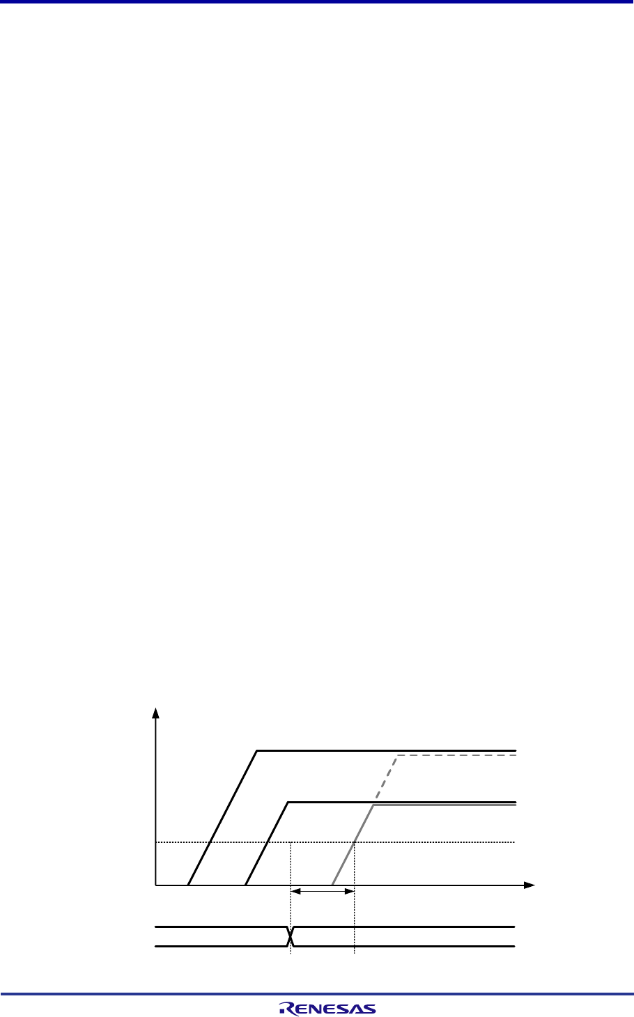
Figure 7 below illustrates the principle behind the DDPC: for a given antenna system an upper and a
lower RSSI threshold can be defined. When the PTX105R operates in high-power mode and the
measured RSSI value drops below the upper threshold, the transmitter is switched to the low-power
mode. Similarly, when in low-power mode and the RSSI exceeds the lower threshold a switch back to
high-power mode is performed. Enough hysteresis between upper and lower switching level ensures a
stable performance.
PTX105R DDPC algorithm is executed on the device, which means that no host-interaction is needed.
Upper THR
Lower THR
RSSI
RF-Field
switch to low-power
switch to high-power
Figure 7: Dynamic Digital Power Control (DDPC)
3.5 Other Supported Features
3.5.1. Over-Temperature Protection
PTX105R features an on-chip temperature sensor that continuously monitors the die temperature. In
case the temperature exceeds a configurable threshold, the transmitter is automatically disabled.
3.5.2. Auxiliary Digital-to-Analog Converter (AUS-DAC)
PTX105R comprises a 5-bit general-purpose digital-to-analog converter (DAC), which operates from
the V
CC
domain and whose output is available at the DAC_O pin.
3.5.3. GPIO Customer Usage
PTX105R provides customer access to 8 GPIOs. This GPIOs can be configured as input or output
separately, depending on the customer application. Specially for system with small MCU, this feature
releases the load on the Host greatly.
3.6 Programmable Control Logic
PTX105R is a highly integrated NFC device greatly unloading the host device in respect to contactless
communication effort. This is achieved by handling major parts of the contactless protocols up to NFC-
Forum ISO-DEP protocol directly on the IC using the Renesas NSC (NFC Soft Controller) interface. On

PTX105R Datasheet
PTX105R Datasheet v1.1
Jun 11, 2024
Page 19
top the SW stacks takes care of data aggregation and management, providing easy to use APIs to the
user.
Timing critical high-level functions, such as ISO-DEP frame de-/composition, automatic frame re-
transmission, WTX handling, EMD handling, etc, are implemented by a programmable control logic
circuit – the on-chip MCU – guaranteeing great execution speed by keeping flexibility by means of
updates/upgrades.
3.6.1. On-chip MCU
The on-chip MCU executes the program downloaded to the PTX105R code-memory. It has access to
all internal status information as well as the configuration mechanisms.
After downloading the micro-code (uCode) the on-chip MCU can be enabled. Subsequently, it accepts
NSC commands for handling all tasks.
3.6.2. PTX105R device control firmware
3.6.2.1. uCode Download Mechanism
Before enabling the on-chip MCU, the devices uCode must be downloaded. This is done via the host-
interface by utilizing the Write-Instruction functionality.
3.6.2.2. Accelerator Enable
Activating the on-chip MCU is achieved by writing the corresponding command to the device.
3.6.2.3. Soft-Reset
PTX105R provides a Soft-Reset functionality that resets all digital blocks and disables all analog blocks
(same condition as after boot).
3.7 Host Interface
PTX105R supports the most used industry standard host interfaces, namely SPI up to 10Mbps, I2C up
to 3.4Mbps and UART with data-rates from 9.6kbps up to 3.4Mbps.
The host interface is designed for typical interface supply voltages used by micro-controllers in the
range of 1.8V to 5V which must be supplied by the host via the VDDIO pin.
3.7.1. Host-Interface Selection
Only one interface type is available at a time and the configuration can only be changed when PTX105R
is in power-down state. Host interface selection is done via the configuration pins SIF1 and SIF2 at
startup. A change of the pin state after boot does not have any effect on the selected interface type.
The following table describes the selection of host interface with respect to the value at the SIF pins:
{SIF2, SIF1}
HIF
2’b00
SPI
2’b01
I2C
2’b10
UART
2’b11
Reserved for test
Table 8: Host Interface Selection
3.7.2. Host-Interface Lines
4 pins (HIF1-HIF4) are utilized for the host interface communication, depending on the selection,
configuration, and application at least 2 HIF pins and up to all 4 are used.

PTX105R Datasheet
PTX105R Datasheet v1.1
Jun 11, 2024
Page 20
Table 9 specifies the pin assignment for the chosen interface type. For SPI, all HIF-interface pins are
used during the communication. In contrast, for I2C HIF1 and HIF2 (corresponding to the ADDR0 and
ADDR1 pins) are only needed at startup to define the last two bits of the I2C-address. For UART mode
HIF1 and HIF2 (CTS and RTS) are used for flow control.
PIN
SPI
I2C
UART
HIF1
NSS
ADDR0
1)
CTS
2)
HIF2
SCK
ADDR1
1)
RTS
2)
HIF3
MOSI
SDA
RXD
HIF4
MISO
SCL
TXD
Table 9: Pin Assignment for HIF Selection
1) LSBs of I2C address, evaluated at boot
2) Flow-control pins
3.7.3. Host Interface Protocol
Above the physical protocol layer, a simple Host-Interface-Protocol is implemented to define the type
and the destination of any host communication.
PTX105R uses different mechanisms for SPI/I2C and UART. For SPI and I2C, the HIP is designed as
a true master-slave protocol where every transaction is initiated by the master (host). The UART
communication on the other hand, is implemented to transfer data to the host directly when needed, i.e.
a data message is immediately initiated without interaction from the host (no IRQ).
To cover the needed functionality, following transaction types are available:
• WInst: Write instruction is used preload the Code Memory (CMEM)
• RMsg: Read a message from PTX105R
• WMsg: Write a message to PTX105R
• WCmd: Write command on PTX105R
The Renesas’ SW stacks use the above-mentioned transactions to provide the functionality to the
application. Hence, direct handling of an interaction with the PTX host interface protocol is usually not
necessary. For more details on the Host Interface Protocol in case needed, please refer to the Host
Interface Reference document.
3.7.4. IRQ
PTX105R has an exclusive IRQ line used to signal the host a communication request.
For SPI and I2C interface asserting an IRQ is the only possibility to initialize a transmission from
PTX105R to the host.
The UART interface in contrast, provides a special “push” mode, allowing PTX105R to initiate a transfer
and transmit notifications to the host directly without the host starting the transfer. This mode is only
usable with hardware flow-control enabled. In this mode, no IRQ line is needed.
3.7.5. SPI
PTX105R implements a standard SPI interface supporting the SPI mode 0 (CPOL = 0, CPHA = 0), i.e.
the clock must be low when data changes and data is captured at the leading clock edge after NSS is
de-asserted.
It uses 4 signal lines for communication:
• Not-Slave-Select (NSS): Active low input to select the device. A communication is initiated by
pulling NSS low. When NSS is high the data output MISO is disabled

PTX105R Datasheet
PTX105R Datasheet v1.1
Jun 11, 2024
Page 21
• Serial Clock (SCK): Clock input for the SPI interface.
• Master-Out-Slave-In (MOSI): Serial data line from host (master) to PTX105R. Data is registered
at positive edge of the clock
• Master-In-Slave-Out (MISO): Serial data line from PTX105R to host (master). Data is shifted on
negative edge of the clock
Figure 8 below illustrates a standard SPI transfer with mode 0. The communication starts on pulling
SCK
1
MOSI
2 43 5 76 8 X
NSS
1
MISO
2 43 5 76 8 X
X
X
t
NSS_setup
t
NSS_hold
Figure 8: SPI mode 0 (CPOL, CPHA = 0)
Data transfers must always be byte aligned, i.e. the number of bits transmitted is a multiple of 8.
Furthermore, the minimum numbers of bytes per frame are 2 (1 header byte + 1 data byte) and frames
must be transmitted at once – without pulling NSS high in between.
Further timing characteristics for SPI interface are specified in Table 10.
Symbol
Parameter
Conditions
Min
Typ
Max
Unit
Remarks
f
SCK
SPI clock
frequency
10
MHz
DC
SCK
SPI clock input
duty cycle
40
50
60
%
t
NSS_setup
25
ns
t
NSS_hold
Hold time from
falling edge of
SCK to NSS high
25
ns
Table 10: SPI Timing Characteristics
3.7.6. I2C
The I2C interface provided by PTX105R is according to the revision 6 of NXP I2C-bus specification.
Following modes are supported by the device:
• Standard-mode (Sm), with a bit rate up to 100 kbps
• Fast-mode (Fm), with a bit rate up to 400 kbps
• Fast-mode Plus (Fm+), with a bit rate up to 1 Mbps
• High-speed mode (Hs-mode), with a bit rate up to 3.4 Mbps
PTX105R supports 7-bit addressing, where the 2 LSBs of the devices I2C-address can be configured
via the pins HIF1 and HIF2 at start-up. In contrast, the upper 5 bits are fixed to 10011(b), resulting in an
address between 0x4C and 0x4F (see Table 11).

PTX105R Datasheet
PTX105R Datasheet v1.1
Jun 11, 2024
Page 22
7bit I2C Address
HIF2 pin
HIF1 pin
0x4C
0
0
0x4D
0
1
0x4E
1
0
0x4F
1
1
Table 11: I2C Address Selection depending on HIF Pin Setting
Clock-stretching is not used by the PTX105R, i.e. no delaying of the communication is necessary.
3.7.7. UART
PTX105R supports serial communication UART communication mode with flow-control up to a data-
rates of 3.4 Mbps. As there is no common clock reference for the UART interface the data-rate reference
must be very accurate.
A transaction starts with a Start-of-Frame (SOF) symbol, i.e. one byte with value 0x55, followed by a
byte indicating the length of transmission payload (TXL). The TXL specifies the number of payload bytes
following. A TXL == 0x00 specifies a length of 256 byte.
Every response from PTX105R starts with the length of reception payload (RXL). As for the
transmission, the RXL specifies the number of bytes to follow, but only values from 1 to 255 are possible.
In case no response is expected (write only transactions) the device sends a one byte acknowledge
putting RXL to 0x00.
After boot, baud-rate detection is enabled and accepts data rates of 9.6kbps or 115.2kbps. Once the
clock system is configured correctly, data rates up to 3.4Mbps can be used.
As mentioned above, hardware flow control (RTS/CTS – both polarities are possible) must be enabled
as TX-push mode is used for communicating with PTX105R.
To further improve communication stability, stop bit can be extended to 2 bits instead of 1 bit.
3.8 FW/SW Functionality
3.8.1. NSC-Interface
To access PTX105R, an optimized high-level software interface is implemented providing functions for
device configuration as well as all data communications.
The interface is based on messages which carry commands, responses, and notifications. Commands
are always sent by the host; responses are generated by the PTX105R as reactions to commands.
Notifications are transmitted by the PTX105R to indicate the host an event has occurred and is usually
asynchronous to commands.
Data packages between PTX105R and the host are called NSC Data messages, and the RF/NFC
specific protocol related header bytes are managed by the on-chip MCU automatically.
3.8.2. SW Split Stack
Renesas provides additional SW-stacks on top of the NSC interface to further ease the integration of
the PTX105R into the target application. The SW stacks manage all interactions with the PTX105R on
NSC level, by setting up and configuring the device, consolidating status information, handling error
messages, and establishing a data channel between the host and the NFC controller.

PTX105R Datasheet
PTX105R Datasheet v1.1
Jun 11, 2024
Page 23
Demos/Example Applications
On-Chip
MCU
NSC
Command
Interpreter
Software
Interface
Commands
Responses
Notifications
Hardware/Platform Abstraction Layer (HAL)
NSC Core Stack Components
RF/Sys Config
PTX Software Stack
PTX105R
Host Processor/Target System
Firmware image
Product APIs + Support Libraries
IoT-API
Figure 9: PTX105R SW Stack Integration View
For more details on the PTX105R SW integration, please refer to the integration manual accordingly.

PTX105R Datasheet
PTX105R Datasheet v1.1
Jun 11, 2024
Page 24
4. Reference Schematic
56 55 54 53
52
51
49
47
46
45
05
06
07
08
09
10
11
12
40
36
35
33
VCC
VCC
VCC
VCC
VCC
VDDIO
D18VD
HIF1
XIN
XOUT
HIF2
HIF3
VCC
VCC
TRXp
TRXp
TRXn
TRXn
VCC
VCC
PTX105R
QFN56
26
HIF4
48
IRQ
SEN
SIF1
SIF2
21
VDDIO
37
HOST µC
Y1
Interface Select
C1
C2
C3
C4
Antenna
C12C11
VCC
C10C9
VCC
C14C13
C17
VDDIO
C16C15
VCC
Figure 10: Exemplary Reference Schematic
Designator
Component type
Component value
Description
C1, C2, C3, C4
Ceramic capacitor
-
Matching capacitors
C9, C11, C13
Ceramic capacitor
10µF
Note that capacitor shall have at least 2.2µF
effective capacitance at applied voltage
C10, C12, C14,
C15, C17
Ceramic capacitor
100nF
C16
Ceramic capacitor
10µF
Optional, depending upon VDDIO supply
noise/impedance
Y1
Crystal oscillator
27.12MHz
According to Table 7
Table 12: Reference Schematic Components

PTX105R Datasheet
PTX105R Datasheet v1.1
Jun 11, 2024
Page 25
5. Ordering and Package Information
5.1 Ordering Information
Part Number
Package
Size (mm)
Shipment Form
Pack Quantity
PTX105RDQ56D13
HVQFN56
7x7
Tape & Reel
3000
Table 13: Ordering Information
5.2 Package Marking
Figure 11: Package Marking Drawing
Symbol
Description
PTX105R
Device Name
XXXXXX.X
Wafer Lot No.
YYWW
Production year/week
Table 14: Marking Code HVQFN56

PTX105R Datasheet
PTX105R Datasheet v1.1
Jun 11, 2024
Page 26
5.3 Package Drawing and Dimension
Figure 12: Package Drawings and Dimensions
